
ASAHI KASEI
[AKD4527B Rev.D]
<KM063700>
- 1 -
'00/9
GENERAL DESCRIPTION
The AKD4527B is an evaluation board for the AK4527B, the Multi-channel Audio CODEC. The
AKD4527B also has the digital audio interface and can achieve the interface with digital audio systems
via opt-connector or BNC connector.
n
Ordering guide
AKD4527B --- Evaluation board for AK4527B
(Cable for connecting with printer port of IBM-AT compatible PC
and control software are packed with this.)
FUNCTION
o
On-board analog input buffer circuit
o
Compatible with 2 types of interface
- DIT(AK4353)/DIR(AK4112A) with optical output/input and BNC input
- Direct interface with AC3 decoder by 10pin header
o
10pin header for serial control interface
Input
Buffer
LIN
RIN
LOUT1
ROUT1
LOUT2
ROUT2
LOUT3
ROUT3
GND
AK4527B
AK4353(DIT)
AK4112A(DIR)
10pin Header
10pin Header
Control Data
BNC In
Opt In
Opt Out
AC3
-15V +15V
Output
Buffer
Regulator
Fig 1. AKD4527B Rev.D Block Diagram
*Circuit diagram and PCB layout are attached at the end of this manual.
Evaluation board Rev.D for AK4527B
AKD4527B

ASAHI KASEI
[AKD4527B Rev.D]
<KM063700>
- 2 -
'00/9
n
Consideration for analog input circuit
AK4527
1nF
470
+
Signal
10k
470
0.1u
22u
4.7k
4.7k
6.25Vpp
1.5Vpp
32
31
30
29
RIN+
RIN-
LIN-
LIN+
4.7k
2.4k
AVDD
4.7k
47u
BIAS
Same circuit
1.5Vpp
NJM5532
+
+
-
-
Op-amp circuit
HPF
LPF
1) Frequency response of HPF
The HPF is implemented on board to cancel the DC offset of analog output of AK4527B.
Frequency response of 1st-order HPF
|Amplitued|
2
= 1/{1+(fc/f)
2
}; fc=1/2
RC=0.7Hz@R=10k,C=22u
fin
20Hz
Frequency Response
-0.006dB
2) Gain and S/N of op-amp circuit
Two stages of inverting op-amp circuit are implemented on board to convert single-ended input to full-differential
input for ADC of AK4527B.
a) Gain
The gain of each op-amp circuit is as following table:
Gain[dB]
First step
-12.40
Second step
0.00
Therefore input level for this board is
-5.51dBV(=1.5Vpp)+12.40dB
= +6.89dBV = 6.25Vpp = 2.21Vrms.
b) S/N (Theory: BW=20k+A)
The output noise level of each op-amp circuit is as following table:
Noise[dBV]
First step
-120.56
Second step
-115.91
The noise level summing differential output of op-amp circuit is
-113.64dBV = -114.13dB (0dB = +0.49dBV = 3Vpp).
S/N of ADC is
104.5dB (measurement).
Therefore total S/N of op-amp circuit and ADC is
104.05dB (measurement: 103.9dB).

ASAHI KASEI
[AKD4527B Rev.D]
<KM063700>
- 3 -
'00/9
3) Frequency response of LPF
1st-order RC LPF is implemented on board to attenuate the noise around the internal sampling frequency of
ADC (64fs=3.072MHz@fs=48kHz)
Frequency response of 1st-order LPF
| Amplitude |
2
= 1/{1+(f/fc)
2
}; fc=1/2
RC=169.3kHz@R=470,C=2000p
(1nF capacitance prior to ADC is doubled because of full-differential input.)
fin
20kHz
40kHz
Frequency Response
-0.060dB
-0.236dB
n
Consideration for analog output circuit
AK4527
22u
Signal
6.0Vpp
28
27
26
25
ROUT1
Same circuit
3.0Vpp
NJM5532
+
-
LOUT1
ROUT2
LOUT2
ROUT3
LOUT3
24
23
Same circuit
Same circuit
Same circuit
Same circuit
10k
4.7k
4.7k
330p
220
1) Frequency response of HPF
The HPF is implemented on board to cancel the DC offset of analog output of AK4527B.
Frequency response of 1st-order HPF
| Amplitude |
2
= 1/{1+(fc/f)
2
}; fc=1/2
RC=0.7Hz@R=10k,C=22u
fin
20Hz
Frequency Response
-0.006dB
2) Gain, S/N and frequency response of op-amp circuit
1st-order filter with non-inverting amp is implemented on board to double the analog output level and attenuate
out-of-band noise.
a) Gain
The gain is
1+4.7k/4.7k = +6.00dB.
Therefore the output level of this board is
0.51dBV(=3.0Vpp) + 6.00dB
= 6.51dBV = 6.0Vpp = 2.12Vrms.
b) S/N (Theory: BW=20k+A)
The output noise level of non-inverting amp
-110.36dBV = -116.87dB (0dB=6.51dBV)
S/N of DAC is
106.0dB (measurement)
Therefore total S/N of op-amp circuit and DAC is
105.66dB (measurement: 105.5dB).

ASAHI KASEI
[AKD4527B Rev.D]
<KM063700>
- 4 -
'00/9
c) Frequency response of filter
Frequency response of the 1st-order filter
| Amplitude |
2
= K*{1+(f/fc
2
)
2
}/{1+(f/fc
1
)
2
};
K = 1+4.7k/4.7k = 2,
fc
1
= 1/2
RC = 102.7kHz@R=4.7k,C=330p,
fc
2
= K*fc
1
= 205.3kHz
Frequency response referenced to output level of this board is as following table:
fin
DC
20kHz
40kHz
80kHz
145kHz
Frequency Response
0dB
-0.121dB
-0.452dB
-1.448dB
-3dB
-6dB
If the frequency response of filter influences the system, 1st-order LPF is also available as the following figure:
AK4527
22u
Signal
6.0Vpp
28
27
26
25
ROUT1
Same circuit
3.0Vpp
NJM5532
+
-
LOUT1
ROUT2
LOUT2
ROUT3
LOUT3
24
23
Same circuit
Same circuit
Same circuit
Same circuit
10k
4.7k
4.7k
3300p
220
LPF
Frequency response of this LPF
| Amplitude |
2
= 1/{1+(f/fc)
2
};
fc = 1/2
RC = 219kHz@R=220,C=3300p
Frequency response referenced to output level of this board is as following table:
fin
DC
20kHz
40kHz
80kHz
219kHz
Frequency Response
0dB
-0.036dB
-0.142dB
-0.543dB
-3dB
-
dB
The total frequency response of this board is sum of the external filter and internal LPF of AK4527B.
These filters are effective to attenuate the high frequency noise since some measurement units is sensitive for
out-of-band noise.

ASAHI KASEI
[AKD4527B Rev.D]
<KM063700>
- 5 -
'00/9
PORT3
uP-I/F
1
2
9
10
CSN
CCLK
CDTI
CDTO
n
Operation sequence
(1) Set up the power supply lines.
[+12V] (orange jack) = +12
+15V
[-12V] (blue jack) = -12
-15V
[AGND] (black jack) = 0V
[DGND] (black jack) = 0V
Each supply line should be distributed from the power supply unit.
�
12V are supplied to analog interface.
+12V is regulated to +5V and +3.3V by regulators(T1,T2).
+5V is supplied to digital interface, AK4527B and TVDD of AK4112A.
+3.3V is supplied to AVDD and DVDD of AK4112A.
(2) Set up the evaluation mode and jumper pins. (See p.3.)
(3) Connect Optical or BNC connector.
[PORT2] (OPT_IN) : Optical input to RX1 of AK4112A
[J10] (RX2) : BNC input to RX1 of AK4112A
(4) Power on.
The AK4527B, AK4112A and AK4353 should be reset once bringing PDN(SW1) "L" upon power-up.
(5) Adjust the interface format
Serial control is needed after the reset by SW1. The default value for interface format of
AK4527B, AK4112A, and AK4353 is "Right justified, 20 bit", "Left justified, 24 bit", and "I
2
S", respectively.
The software "4527.exe" packed with the AKD4527B is used for the set-up of the AK4527B.
Evaluation mode 1 : DIF1-0 bit of the AK4527B should be set to "11" .
Evaluation mode 2, 3: DIF1-0 bit of the AK4527B should be set to "10".
Evaluation mode 4 : AK4112A and AK4527B should be set to adjust the format of DSP.
(6) Set up software.
The control mode of AK4527B and AK4112A is fixed to "serial".
The AKD4527B can be controlled via the printer port (parallel port) of IBM-AT
compatible PC. Connect PORT3(uP-I/F) with PC by 10-line flat cable
packed with the AKD4527B.
Take care of the direction of connector. There is a mark at pin#1.
The pin layout of PORT3 is as Figure 2. Figure 2. PORT3 pin layout
ASAHI KASEI
[AKD4527B Rev.D]
<KM063700>
- 6 -
'00/9
n
Evaluation mode
1) Evaluation of ADC
TOTX176 is used for digital output. Clock mode of the AK4112A should be set to PLL mode or X'tal mode.
2) Evaluation of DAC
TORX176 or BNC is used for digital input. Clock mode of the AK4112A should be set to PLL mode. "4112" should
be selected on JP4,5 and 6.
3) Loopback mode
Clock mode of the AK4112A should be set to PLL mode or X'tal mode. "4112" should be selected on JP4,5 and 6.
4) Evaluation of DAC using DSP
"DSP" should be selected on JP4,5 and 6.
Evaluation mode
AK4112A clock set-up
JP4,5,6
Used I/F
ADC
CM1="0", CM0="0"(PLL mode) or
CM1="0", CM0="1"(X'tal mode)
Don't
care
TOTX176
optical output
DAC
CM1="0", CM0="0"(PLL mode)
"4112"
Loopback
CM1="0", CM0="1"(X'tal mode)
"4112"
Using DSP
CM1="0", CM0="0"(PLL mode)
"DSP"
PORT5(10-pin Header)
Table 2.Evalution mode
n
Jumper pin set up
[JP1] (GND) ---Analog GND and Digital GND
[JP4,5,6] (SDTI1,2,3) --- AK4527B SDTI1,2,3 input source select
<DSP> : Serial Data is input from DSP via PORT5.
<4112> : Serial Data is input from AK4112A SDTO. <default>
[JP2] (V/TX) --- AK4112A V/TX output select.
<V> : Validity. <default>
<TX> : Transmit channel (through data)
n
The function of the toggle SW.
[SW1] : Resets the AK4527B, AK4112A and AK4353. Keep "H" during normal operation.
n
The indication content for LED.
[LE1] (ERF) : AK4112A unlock and parity error output.
[LE2] (FS96) : AK4112A 96kHz sampling detect.
[LE3] (AUTO) : AK4112A AC-3/MPEG detect.
[LE4] (V) : Validity

ASAHI KASEI
[AKD4527B Rev.D]
<KM063700>
- 7 -
'00/9
MEASUREMENT RESULTS
1) ADC part
[Measurement condition]
�
Measurement unit : Audio Precision, System two, Cascade
�
MCLK : 256fs
�
BICK : 64fs
�
fs : 44.1kHz
�
BW : 10Hz
20kHz(fs=44.1kHz), 10Hz
48kHz(fs=96kHz)
�
Bit : 24bit
�
Power Supply : AVDD=DVDD=TVDD=5V
�
Analog Input : Differential
�
Interface : DIT
�
Temperature : Room
fs=44.1kHz
Parameter
Input signal
Measurement filter
Results
S/(N+D)
1kHz, -0.5dB 20kLPF
96.2dB
DR
1kHz, -60dB
20kLPF, A-weighted
103.3dB
S/N
no signal
20kLPF, A-weighted
103.9dB
fs=96kHz
Parameter
Input signal
Measurement filter
Results
S/(N+D)
1kHz, -0.5dB fs/2
86.7dB
DR
1kHz, -60dB
fs/2, A-weighted
102.9dB
S/N
no signal
fs/2, A-weighted
103.4dB
ASAHI KASEI
[AKD4527B Rev.D]
<KM063700>
- 8 -
'00/9
2) DAC part
[Measurement condition]
�
Measurement unit : Audio Precision, System two, Cascade
�
MCLK : 256fs
�
BICK : 64fs
�
fs : 44.1kHz, 96kHz
�
BW : 10Hz
22kHz (fs=44.1kHz), 10Hz
40kHz (fs=96kHz)
�
Bit : 24bit
�
Power Supply : AVDD=DVDD=TVDD=5V
�
Analog Input : Differential
�
Interface : DIR
�
Temperature : Room
fs=44.1kHz
Parameter
Input signal
Measurement filter
Results
S/(N+D)
1kHz, 0dB
20kLPF
97.3dB
DR
1kHz, -60dB
22kLPF, A-weighted
105.1dB
S/N
"0"data
22kLPF, A-weighted
105.5dB
fs=96kHz
Parameter
Input signal
Measurement filter
Results
S/(N+D)
1kHz, 0dB
40kLPF
96.2dB
40kLPF
100.5dB
DR
1kHz, -60dB
22kLPF, A-weighted
104.9dB
40kLPF
100.6dB
S/N
"0"data
22kLPF, A-weighted
104.9dB

ASAHI KASEI
[AKD4527B Rev.D]
<KM063700>
- 9 -
'00/9
1.ADC
(ADC fs=44.1kHz)
AKM
AK4527 FFT (Input Level=-0.5dBFS,fin=1kHz)
20
20k
50
100
200
500
1k
2k
5k
10k
Hz
-160
+ 0
-150
-140
-130
-120
-110
-100
-90
-80
-70
-60
-50
-40
-30
-20
-10
d
B
F
S
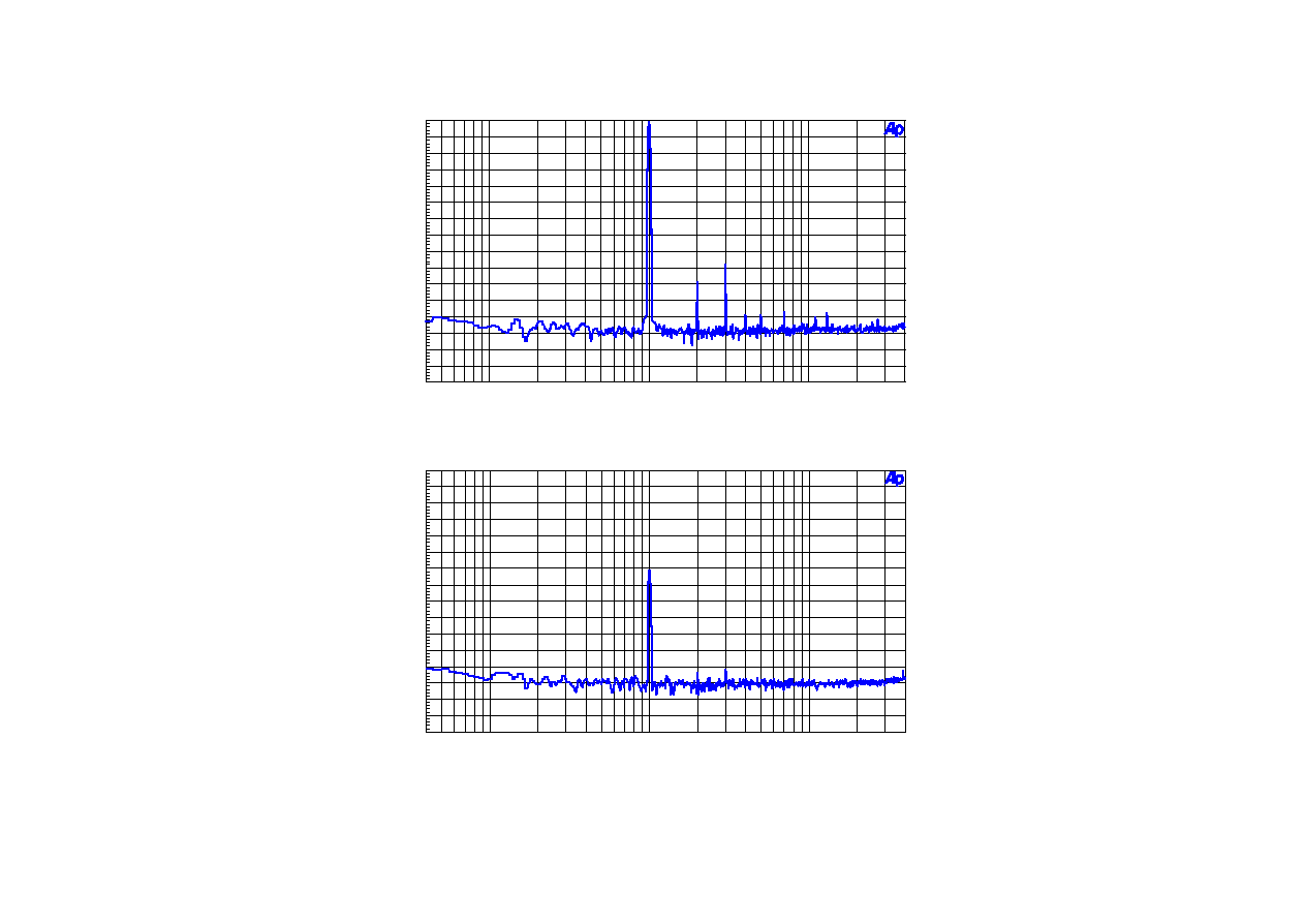
FFT (Input=-0.5dBFS, fin=1kHz)
AKM
AK4527 FFT(Level=-60dBFS, fin=1kHz)
20
20k
50
100
200
500
1k
2k
5k
10k
Hz
-160
+ 0
-150
-140
-130
-120
-110
-100
-90
-80
-70
-60
-50
-40
-30
-20
-10
d
B
F
S
FFT (Input=-60dBFS, fin=1kHz)

ASAHI KASEI
[AKD4527B Rev.D]
<KM063700>
- 10 -
'00/9
(ADC fs=44.1kHz)
AKM
AK4527 FFT(noise floor)
20
20k
50
100
200
500
1k
2k
5k
10k
Hz
-160
+ 0
-150
-140
-130
-120
-110
-100
-90
-80
-70
-60
-50
-40
-30
-20
-10
d
B
F
S
FFT (noise floor)
ASAHI KASEI
[AKD4527B Rev.D]
<KM063700>
- 11 -
'00/9
(ADC fs=44.1kHz)
AKM
AK4527 THD + N vs Amplitude(fin=1kHz)
-140
+ 0
-130
-120
-110
-100
-90
-80
-70
-60
-50
-40
-30
-20
-10
dBr
-110
-90
-109
-108
-107
-106
-105
-104
-103
-102
-101
-100
-99
-98
-97
-96
-95
-94
-93
-92
-91
d
B
F
S
THD + N vs Amplitude (fin=1kHz)
AKM
AK4527 THD + N vs Input Frequency(Input Level=-0.5dBFS)
20
20k
50
100
200
500
1k
2k
5k
10k
Hz
-110
-80
-108
-106
-104
-102
-100
-98
-96
-94
-92
-90
-88
-86
-84
-82
d
B
F
S
THD + N vs Input Frequency (Input=-0.5dBFS)

ASAHI KASEI
[AKD4527B Rev.D]
<KM063700>
- 12 -
'00/9
(ADC fs=44.1kHz)
AKM
AK4527 Linearity
-140
+ 0
-130
-120
-110
-100
-90
-80
-70
-60
-50
-40
-30
-20
-10
dBr
-140
+ 0
-130
-120
-110
-100
-90
-80
-70
-60
-50
-40
-30
-20
-10
d
B
F
S
Linearity(fin=1kHz)
AKM
AK4527 Linearity
20
20k
50
100
200
500
1k
2k
5k
10k
Hz
-1
+ 0
-0.95
-0.9
-0.85
-0.8
-0.75
-0.7
-0.65
-0.6
-0.55
-0.5
-0.45
-0.4
-0.35
-0.3
-0.25
-0.2
-0.15
-0.1
-0.05
d
B
F
S
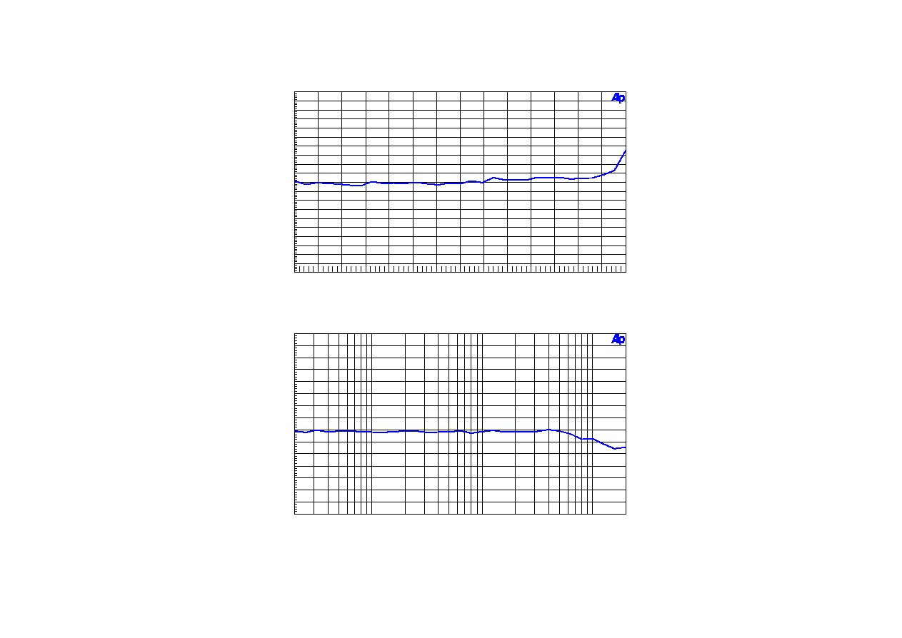
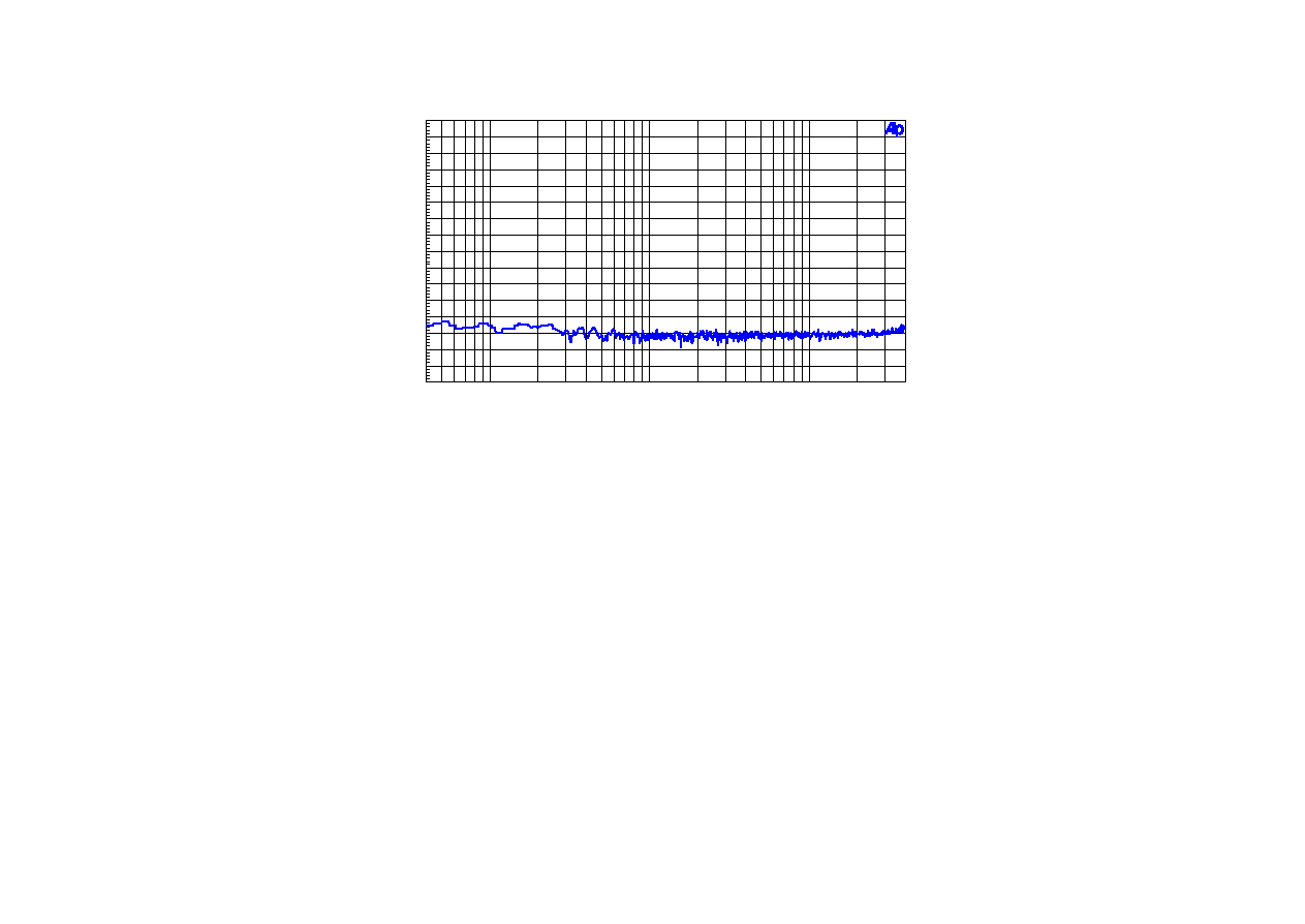
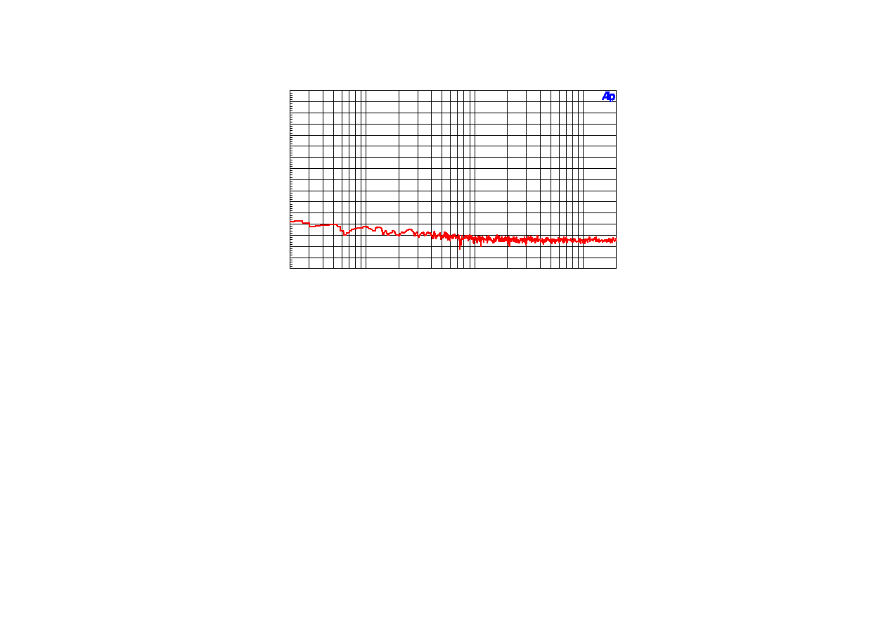
Frequency Response(Input Level=-0.5dBFS)
(including input RC filter)

ASAHI KASEI
[AKD4527B Rev.D]
<KM063700>
- 13 -
'00/9
(ADC fs=44.1kHz)
AKM
AK4527 Crosstalk
20
20k
50
100
200
500
1k
2k
5k
10k
Hz
-130
-100
-128
-126
-124
-122
-120
-118
-116
-114
-112
-110
-108
-106
-104
-102
d
B
F
S
Crosstalk (Upper = Rch, Lower = Lch)
ASAHI KASEI
[AKD4527B Rev.D]
<KM063700>
- 14 -
'00/9
(ADC fs=96kHz)
AKM
AK4527 FFT (Input Level=-0.5dBFS,fin=1kHz)
40
40k
50
100
200
500
1k
2k
5k
10k
20k
Hz
-160
+ 0
-150
-140
-130
-120
-110
-100
-90
-80
-70
-60
-50
-40
-30
-20
-10
d
B
F
S
FFT(Input=-0.5dBFS, fin=1kHz)
AKM
AK4527 FFT (Input Level=-60dBFS,fin=1kHz)
40
40k
50
100
200
500
1k
2k
5k
10k
20k
Hz
-160
+ 0
-150
-140
-130
-120
-110
-100
-90
-80
-70
-60
-50
-40
-30
-20
-10
d
B
F
S
FFT(Input=-60dBFS, fin=1kHz)
ASAHI KASEI
[AKD4527B Rev.D]
<KM063700>
- 15 -
'00/9
(ADC fs=96kHz)
AKM
AK4527 FFT (noise floor)
40
40k
50
100
200
500
1k
2k
5k
10k
20k
Hz
-160
+ 0
-150
-140
-130
-120
-110
-100
-90
-80
-70
-60
-50
-40
-30
-20
-10
d
B
F
S
FFT(Input = noise floor)
ASAHI KASEI
[AKD4527B Rev.D]
<KM063700>
- 16 -
'00/9
AKM
AK4527 THD + N vs Amplitude(fin=1kHz)
-140
+ 0
-130
-120
-110
-100
-90
-80
-70
-60
-50
-40
-30
-20
-10
dBr
-110
-80
-108
-106
-104
-102
-100
-98
-96
-94
-92
-90
-88
-86
-84
-82
d
B
F
S
THD + N vs Amplitude(fin=1kHz)
AKM
AK4527 THD + N vs Input Frequency(Input Level=-0.5dBFS)
40
40k
50
100
200
500
1k
2k
5k
10k
20k
Hz
-100
-70
-98
-96
-94
-92
-90
-88
-86
-84
-82
-80
-78
-76
-74
-72
d
B
F
S
THd + N vs Input Frequency(Input Level=-0.5dBFS)

ASAHI KASEI
[AKD4527B Rev.D]
<KM063700>
- 17 -
'00/9
AKM
AK4527 Linearity
-140
+ 0
-130
-120
-110
-100
-90
-80
-70
-60
-50
-40
-30
-20
-10
dBr
-140
+ 0
-130
-120
-110
-100
-90
-80
-70
-60
-50
-40
-30
-20
-10
d
B
F
S
Linearity(fin=1kHz)
AKM
AK4527 Crosstalk
40
40k
50
100
200
500
1k
2k
5k
10k
20k
Hz
-1
+ 0
-0.95
-0.9
-0.85
-0.8
-0.75
-0.7
-0.65
-0.6
-0.55
-0.5
-0.45
-0.4
-0.35
-0.3
-0.25
-0.2
-0.15
-0.1
-0.05
d
B
F
S
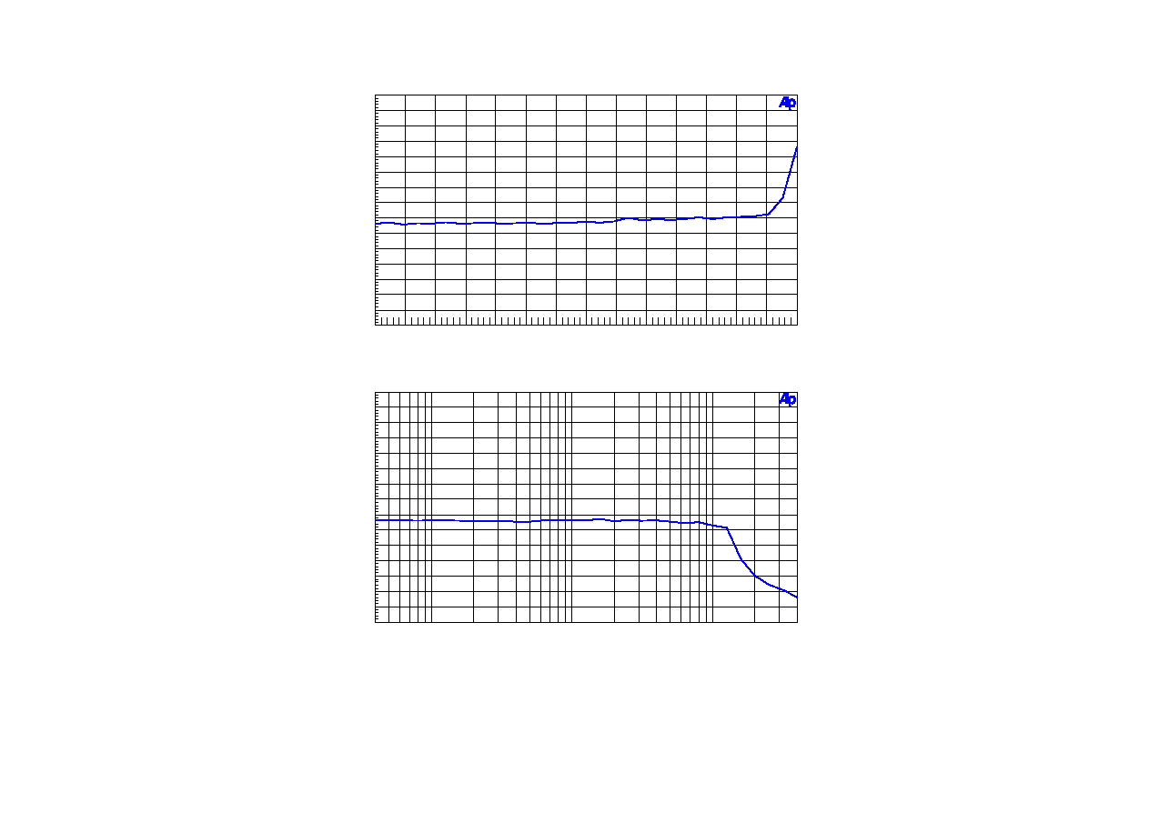
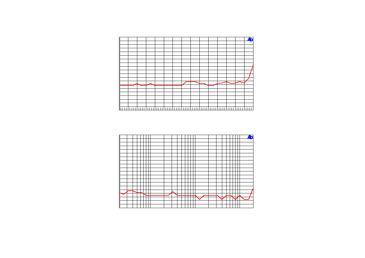
Frequency Response(Input Level=-0.5dBFS)
(including input RC filter)

ASAHI KASEI
[AKD4527B Rev.D]
<KM063700>
- 18 -
'00/9
AKM
AK4527 Crosstalk
40
40k
50
100
200
500
1k
2k
5k
10k
20k
Hz
-130
-90
-128
-126
-124
-122
-120
-118
-116
-114
-112
-110
-108
-106
-104
-102
-100
-98
-96
-94
-92
d
B
F
S
Crosstalk (Upper = Rch, Lower = Lch)

ASAHI KASEI
[AKD4527B Rev.D]
<KM063700>
- 19 -
'00/9
2.DAC
(DAC fs=44.1kHz)
AKM
AK4527 DAC FFT (Input Level=0dBFS, fin=1kHz)
20
20k
50
100
200
500
1k
2k
5k
10k
Hz
-160
+ 0
-150
-140
-130
-120
-110
-100
-90
-80
-70
-60
-50
-40
-30
-20
-10
d
B
r
A
FFT (Input=0dBFS, fin=1kHz)
AKM
AK4527 DAC FFT (Input Level=-60dBFS, fin=1kHz)
20
20k
50
100
200
500
1k
2k
5k
10k
Hz
-160
+ 0
-150
-140
-130
-120
-110
-100
-90
-80
-70
-60
-50
-40
-30
-20
-10
d
B
r
A
FFT (Input=-60dBFS, fin=1kHz)
ASAHI KASEI
[AKD4527B Rev.D]
<KM063700>
- 20 -
'00/9
(DAC fs=44.1kHz)
AKM
AK4527 DAC FFT (Input 0data)
20
20k
50
100
200
500
1k
2k
5k
10k
Hz
-160
+ 0
-150
-140
-130
-120
-110
-100
-90
-80
-70
-60
-50
-40
-30
-20
-10
d
B
r
A
FFT (Input="0"data)
ASAHI KASEI
[AKD4527B Rev.D]
<KM063700>
- 21 -
'00/9
(DAC fs=44.1kHz)
AKM
AK4527 DAC THD + N vs Amplitude(fin=1kHz)
-150
+ 0
-140
-130
-120
-110
-100
-90
-80
-70
-60
-50
-40
-30
-20
-10
dBFS
-110
-90
-109
-108
-107
-106
-105
-104
-103
-102
-101
-100
-99
-98
-97
-96
-95
-94
-93
-92
-91
d
B
r
A
THD + N vs Amplitude(fin=1kHz)
AKM
AK4527 DAC THD + N vs Input Frequency(Input Level=0dBFS)
20
20k
50
100
200
500
1k
2k
5k
10k
Hz
-100
-80
-99
-98
-97
-96
-95
-94
-93
-92
-91
-90
-89
-88
-87
-86
-85
-84
-83
-82
-81
d
B
r
A
THD + N vs Input Frequency (Input=0dBFS)

ASAHI KASEI
[AKD4527B Rev.D]
<KM063700>
- 22 -
'00/9
(DAC fs=44.1kHz)
AKM
AK4527 DAC Linearity
-150
+ 0
-140
-130
-120
-110
-100
-90
-80
-70
-60
-50
-40
-30
-20
-10
dBFS
-150
+ 0
-140
-130
-120
-110
-100
-90
-80
-70
-60
-50
-40
-30
-20
-10
d
B
r
A
Linearity(fin=1kHz)
AKM
AK4527 DAC Frequency Response
2k
20k
4k
6k
8k
10k
12k
14k
16k
18k
Hz
-0.5
+0.5
-0.45
-0.4
-0.35
-0.3
-0.25
-0.2
-0.15
-0.1
-0.05
+ 0
+0.05
+0.1
+0.15
+0.2
+0.25
+0.3
+0.35
+0.4
+0.45
d
B
r
A
Frequency Response(Input Level=0dBFS)
(including external RC filter)
ASAHI KASEI
[AKD4527B Rev.D]
<KM063700>
- 23 -
'00/9
(DAC fs=44.1kHz)
AKM
AK4527 DAC Crosstalk
20
20k
50
100
200
500
1k
2k
5k
10k
Hz
-120
-90
-118
-116
-114
-112
-110
-108
-106
-104
-102
-100
-98
-96
-94
-92
d
B
r
A
Crosstalk(Upper=Rch, Lower=Lch)

ASAHI KASEI
[AKD4527B Rev.D]
<KM063700>
- 24 -
'00/9
(DAC fs=96kHz)
AKM
AK4527 FFT (Input Level=0dBFS, fin=1kHz, notch)
40
40k
50
100
200
500
1k
2k
5k
10k
20k
Hz
-160
+ 0
-150
-140
-130
-120
-110
-100
-90
-80
-70
-60
-50
-40
-30
-20
-10
d
B
r
A
FFT (Input=0dBFS, fin=1kHz, Notch)
AKM
AK4527 FFT (Input Level=-60dBFS, fin=1kHz)
40
40k
50
100
200
500
1k
2k
5k
10k
20k
Hz
-160
+ 0
-150
-140
-130
-120
-110
-100
-90
-80
-70
-60
-50
-40
-30
-20
-10
d
B
r
A
FFT (Input=-60dBFS,fin=1kHz)
ASAHI KASEI
[AKD4527B Rev.D]
<KM063700>
- 25 -
'00/9
(DAC fs=96kHz)
AKM
AK4527 FFT (Input="0" data)
40
40k
50
100
200
500
1k
2k
5k
10k
20k
Hz
-160
+ 0
-150
-140
-130
-120
-110
-100
-90
-80
-70
-60
-50
-40
-30
-20
-10
d
B
r
A
FFT (Input="0"data)
AKM
AK4527 THD + N vs Amplitude (fin=1kHz)
-140
+ 0
-130
-120
-110
-100
-90
-80
-70
-60
-50
-40
-30
-20
-10
dBFS
-110
-80
-108
-106
-104
-102
-100
-98
-96
-94
-92
-90
-88
-86
-84
-82
d
B
r
A
THD + N vs Amplitude (fin=1kHz)
ASAHI KASEI
[AKD4527B Rev.D]
<KM063700>
- 26 -
'00/9
(DAC fs=96kHz)
AKM
AK4527 THD + N vs Input Frequency (Input Frequency)
40
40k
50
100
200
500
1k
2k
5k
10k
20k
Hz
-110
-80
-108
-106
-104
-102
-100
-98
-96
-94
-92
-90
-88
-86
-84
-82
d
B
r
A
THD + N vs Input Frequency (Input=0dBFS)
AKM
AK4527 Linearity
-140
+ 0
-130
-120
-110
-100
-90
-80
-70
-60
-50
-40
-30
-20
-10
dBFS
-140
+ 0
-130
-120
-110
-100
-90
-80
-70
-60
-50
-40
-30
-20
-10
d
B
r
A
Linearity(fin=1kHz)
ASAHI KASEI
[AKD4527B Rev.D]
<KM063700>
- 27 -
'00/9
(DAC fs=96kHz)
AKM
AK4527 Frequency Response
2.5k
40k
5k
7.5k
10k
12.5k
15k
17.5k
20k
22.5k
25k
27.5k
30k
32.5k
35k
37.5k
Hz
-1
+0.5
-0.9
-0.8
-0.7
-0.6
-0.5
-0.4
-0.3
-0.2
-0.1
+ 0
+0.1
+0.2
+0.3
+0.4
d
B
r
A
Frequency Response(Input Level=0dBFS)
(including external RC filter)
AKM
AK4527 Crosstalk
40
40k
50
100
200
500
1k
2k
5k
10k
20k
Hz
-130
-90
-128
-126
-124
-122
-120
-118
-116
-114
-112
-110
-108
-106
-104
-102
-100
-98
-96
-94
-92
d
B
r
A
Crosstalk (Upper=Rch, Lower=Lch)

ASAHI KASEI
[AKD4527B Rev.D]
<KM063700>
- 28 -
'00/9
IMPORTANT NOTICE
�
These products and their specifications are subject to change without notice. Before considering any use or
application, consult the Asahi Kasei Microsystems Co., Ltd. (AKM) sales office or authorized distributor
concerning their current status.
�
AKM assumes no liability for infringement of any patent, intellectual property, or other right in the application or
use of any information contained herein.
�
Any export of these products, or devices or systems containing them, may require an export license or other
official approval under the law and regulations of the country of export pertaining to customs and tariffs,
currency exchange, or strategic materials.
�
AKM products are neither intended nor authorized for use as critical components in any safety, life support, or
other hazard related device or system, and AKM assumes no responsibility relating to any such use, except with
the express written consent of the Representative Director of AKM. As used here:
(a) A hazard related device or system is one designed or intended for life support or maintenance of safety or
for applications in medicine, aerospace, nuclear energy, or other fields, in which its failure to function or
perform may reasonably be expected to result in loss of life or in significant injury or damage to person or
property.
(b) A critical component is one whose failure to function or perform may reasonably be expected to result,
whether directly or indirectly, in the loss of the safety or effectiveness of the device or system containing it,
and which must therefore meet very high standards of performance and reliability.
�
It is the responsibility of the buyer or distributor of an AKM product who distributes, disposes of, or otherwise
places the product with a third party to notify that party in advance of the above content and conditions, and the
buyer or distributor agrees to assume any and all responsibility and liability for and hold AKM harmless from any
and all claims arising from the use of said product in the absence of such notification.

ASAHI KASEI
[AK4527B Control Program]
`00/9
- 1 -
AK4527B Control Program operation manual
1.
Connect IBM-AT compatible PC with Eva-board by 10-line type flat cable (packed with Eva-board).
Take care of the direction of 10pin Header (Refer to manual of Eva-board).
2.
Start up "WINDOWS 95" or "WINDOWS 98".
3.
Insert the floppy-disk packed with Eva-board into the floppy-disk drive.
4.
Set up "MS-DOS" from start menu.
5.
Change directory to the floppy-disk drive(ex.a:) at MS-DOS prompt.
6.
Type "4527b".
7.
Then follow the displayed comment (See the following).
==================== <<Operating flow>> =====================
Write data/ Display register map/ Reset etc.� loop
=========================================================

ASAHI KASEI
[AK4527B Control Program]
`00/9
- 2 -
At first the following message is displayed:
****** AK4527B Control Program ver 2.0 , '00/9 ******
copyright(c) 2000, Asahi Kasei Microsystems co.,ltd.
All rights reserved.
Then the following default register map is displayed (Loop starts from here):
AK4527B : 3-wire Serial control mode CAD1-0=01 ----------------------------
ADDR = 00 : 00 <Control 1> ( 0 0 0 0 DIF1 DIF0 0 SMUTE)
ADDR = 01 : 00 <Control 2> ( 0 0 LOOP1 LOOP0 SDOS DFS ACKS 0 )
ADDR = 02 : 00 <L1 ATT> ( ATT7 ATT6 ATT5 ATT4 ATT3 ATT2 ATT1 ATT0 )
ADDR = 03 : 00 <R1 ATT> ( ATT7 ATT6 ATT5 ATT4 ATT3 ATT2 ATT1 ATT0 )
ADDR = 04 : 00 <L2 ATT> ( ATT7 ATT6 ATT5 ATT4 ATT3 ATT2 ATT1 ATT0 )
ADDR = 05 : 00 <R2 ATT> ( ATT7 ATT6 ATT5 ATT4 ATT3 ATT2 ATT1 ATT0 )
ADDR = 06 : 00 <L3 ATT> ( ATT7 ATT6 ATT5 ATT4 ATT3 ATT2 ATT1 ATT0 )
ADDR = 07 : 00 <R3 ATT> ( ATT7 ATT6 ATT5 ATT4 ATT3 ATT2 ATT1 ATT0 )
ADDR = 08 : 00 <DEM> ( 0 0 DEMA1 DEMA0 DEMB1 DEMB0 DEMC1 DEMC0)
ADDR = 09 : 01 <CLK Mode> ( 0 0 0 0 0 0 0 RSTN )
ADDR = 0A : 3F <DZF> ( OVFE 0 DZFM2 DZFM1 DZFM0 PWVRN PWADN PWDAN)
Input 1(Write), R(Reset), T(Table), I(Increment) or D(Decrement) :
1) If you input "1", you can write data to AK4527B.
You can write data to AK4527B
Input Register Address (2 figure, hex) (00-0A) =
Input register address in 2 figures of hexadecimal.
Then current data of this address is displayed:
AK4527B
ADDR = 00 : 08 <Control 1> ( 0 0 0 0 DIF1 DIF0 0 SMUTE)
0 0 0 0 1 0 0 0
Input Register Data (2 figure, hex) (00-FF) =
You can write control data to this address. Input control data in 2 figures of hexadecimal.
Refer to datasheet of AK4527B.
Then the data written to this address is displayed:
AK4527B
ADDR = 00 : 0C <Control 1> ( 0 0 0 0 DIF1 DIF0 0 SMUTE)
0 0 0 0 1 1 0 0
2) If you input "R" or "r", this program writes default data to all register addresses.
3) If you input "T" or "t", current register map is displayed.
4) If you input "I" or "i", this program increment data of current address by 1.
5) If you input "D" or "d", this program decrement data of current address by 1.
6) If you input "S" or "s", this program is terminated.

ASAHI KASEI
[AK4112A Control Program]
`00/2
- 1 -
AK4112A Control Program operation manual
1. Connect IBM-AT compatible PC with Eva-board by 10-line type flat cable (packed with Eva-board).
Take care of the direction of 10pin Header (Refer to manual of Eva-board).
2. Start up "WINDOWS 95" or "WINDOWS 98".
3. Insert the floppy-disk packed with Eva-board into the floppy-disk drive.
4. Set up "MS-DOS" from start menu.
5. Change directory to the floppy-disk drive(ex.a:) at MS-DOS prompt.
6. Type "4112".
7. Then follow the displayed comment (See the following).
==================== <<Operating flow>> =====================
Write data/ Display register map/ Reset etc.� loop
=========================================================

ASAHI KASEI
[AK4112A Control Program]
`00/2
- 2 -
At first the following message is displayed:
****** AK4112 Control Program ver 2.0 , '00/1 ******
copyright(c) 2000, Asahi Kasei Microsystems co.,ltd.
All rights reserved.
Then the following is displayed:
After chip address is defined, the following default register map is displayed (Loop starts from here):
AK4112 Register Map
ADDR = 00 : 03 <CLK PD ctrl> (0 BCU CM1 CM0 OCKS1 OCKS0 PWN RSTN )
ADDR = 01 : 80 <I/O ctrl> (MPAR MTSC CS12 XTE IPS1 IPS0 OPS1 OPS0 )
ADDR = 02 : 4A <FMT DM ctrl> (V/TX DIF2 DIF1 DIF0 DEAU DEM1 DEM0 DFS )
ADDR = 03 : 00 <RCV STAT 1> (ERF 0 AUDIO AUTO PEM FS1 FS0 RFS96)
ADDR = 04 : 00 <RCV STAT 2> (CV STC CRC UNLOCK V FRERR BIP PAR )
ADDR = 05 : 00 <ChA STAT 0> (CA7 CA6 CA5 CA4 CA3 CA2 CA1 CA0 )
ADDR = 06 : 00 <ChA STAT 1> (CA15 CA14 CA13 CA12 CA11 CA10 CA9 CA8 )
ADDR = 07 : 00 <ChA STAT 2> (CA23 CA22 CA21 CA20 CA19 CA18 CA17 CA16)
ADDR = 08 : 00 <ChA STAT 3> (CA31 CA30 CA29 CA28 CA27 CA26 CA25 CA24)
ADDR = 09 : 00 <ChB STAT 0> (CB7 CB6 CB5 CB4 CB3 CB2 CB1 CB0 )
ADDR = 0A : 00 <ChB STAT 1> (CB15 CB14 CB13 CB12 CB11 CB10 CB9 CB8 )
ADDR = 0B : 00 <ChB STAT 2> (CB23 CB22 CB21 CB20 CB19 CB18 CB17 CB16)
ADDR = 0C : 00 <ChB STAT 3> (CB31 CB30 CB29 CB28 CB27 CB26 CB25 CB24)
ADDR = 0D : 00 <BstPre Pc 0> (PC7 PC6 PC5 PC4 PC3 PC2 PC1 PC0 )
ADDR = 0E : 00 <BstPre Pc 1> (PC15 PC14 PC13 PC12 PC11 PC10 PC9 PC8 )
ADDR = 0F : 00 <BstPre Pd 0> (PD7 PD6 PD5 PD4 PD3 PD2 PD1 PD0 )
ADDR = 10 : 00 <BstPre Pd 1> (PD15 PD14 PD13 PD12 PD11 PD10 PD9 PD8 )
ADDR = 11 : 02 <Count ctrl> (0 0 0 0 0 EFH1 EFH0 XFS96)
Input 0(Read), 1(Write), R(Reset), T(Table) or S(Stop) :
1) If you input "0", you can read data from AK4112A.
You can read data from AK4112
Input Register Address (2 figure, hex) (00H-11H) =
Input register address in 2 figures of hexadecimal.
Then current data of this address is displayed:
AK4112A
ADDR = 00 : 03 <CLK PD ctrl> (0 BCU CM1 CM0 OCKS1 OCKS0 PWN RSTN)
0 0 0 0 0 0 1 1
2) If you input "1", you can write data to AK4112A.
You can write data to AK4112
Input Register Address (2 figure, hex) (00H-02H or 11H) =
Input register address in 2 figures of hexadecimal.
Then current data of this address is displayed:
AK4112A
ADDR = 00 : 03 <CLK PD ctrl> (0 BCU CM1 CM0 OCKS1 OCKS0 PWN RSTN)
0 0 0 0 0 0 1 1
Input Register Data (2 figure, hex) =
You can write control data to this address. Input control data in 2 figures of hexadecimal.
Refer to datasheet of AK4112A.
Then the data written to this address is displayed:
AK4112
ADDR = 00 : 23 <CLK PD ctrl> (0 BCU CM1 CM0 OCKS1 OCKS0 PWN RSTN)
0 0 1 0 0 0 1 1
3) If you input "R" or "r", this program writes default data to all register addresses.
4) If you input "T" or "t", current register map is displayed.
5) If you input "S" or "s", this program is terminated.

ASAHI KASEI
[AK4353 Control Program]
`00/2
- 1 -
AK4353 Control Program operation manual
1.
Connect IBM-AT compatible PC with Eva-board by 10-line type flat cable (packed with Eva-board).
Take care of the direction of 10pin Header (Refer to manual of Eva-board).
2.
Start up "WINDOWS 95" or "WINDOWS 98".
3.
Insert the floppy-disk packed with Eva-board into the floppy-disk drive.
4.
Set up "MS-DOS" from start menu.
5.
Change directory to the floppy-disk drive(ex.a:) at MS-DOS prompt.
6.
Type "4353".
7.
Then follow the displayed comment (See the following).
==================== <<Operating flow>> =====================
Write data/ Display register map/ Reset etc.� loop
=========================================================

ASAHI KASEI
[AK4353 Control Program]
`00/2
- 2 -
At first the following message is displayed:
****** AK4353 Control Program ver 3.0 , '00/2 ******
copyright(c) 2000, Asahi Kasei Microsystems co.,ltd.
All rights reserved.
Then the following default register map is displayed (Loop starts from here):
3-wire Serial control mode CAD1-0=11 ------------------------------------
ADDR = 00 : 0B <Control 1> ( 0 0 0 0 DIF2 DIF1 DIF0 RSTN )
ADDR = 01 : 01 <Control 2> ( 0 0 DFS1 DFS0 CKS2 CKS1 CKS0 RSTN )
ADDR = 02 : 94 <Control 3> ( PL3 PL2 PL1 PL0 DEM1 DEM0 ATC SMUTE)
ADDR = 03 : FF <Lch ATT> ( ATT7 ATT6 ATT5 ATT4 ATT3 ATT2 ATT1 ATT0 )
ADDR = 04 : FF <Rch ATT> ( ATT7 ATT6 ATT5 ATT4 ATT3 ATT2 ATT1 ATT0 )
ADDR = 05 : 00 <TX> ( 0 0 0 0 0 0 V TXE )
ADDR = 06 : 00 <Ch Status 1>( 0 CS29 CS28 CS24 CS3 CS2 CS2 CS1 )
ADDR = 07 : 04 <Ch Status 2>( CS15 CS14 CS13 CS12 CS11 CS10 CS9 CS8 )
Input 1(Write), R(Reset), T(Table), I(Increment), D(Decrement) or S(Stop) :
1) If you input "1", you can write data to AK4353.
You can write data to AK4353
Input Register Address (2 figure, hex) (00-07) =
Input register address in 2 figures of hexadecimal.
Then current data of this address is displayed:
ADDR = 00 : 0B <Control 1> ( 0 0 0 0 DIF2 DIF1 DIF0 RSTN )
0 0 0 0 1 0 1 1
Input Register Data (2 figure, hex) (00-FF) =
You can write control data to this address. Input control data in 2 figures of hexadecimal.
Refer to datasheet of AK4353.
Then the data written to this address is displayed:
ADDR = 00 : 09 <Control 1> ( 0 0 0 0 DIF2 DIF1 DIF0 RSTN )
0 0 0 0 1 0 0 1
2) If you input "R" or "r", this program writes default data to all register addresses.
3) If you input "T" or "t", current register map is displayed.
4) If you input "I" or "i", this program increment data of current address by 1 (only for addr=03H or 04H). You can
increment ATT value by 1step.
5) If you input "D" or "d", this program decrement data of current address by 1 (only for addr=03H or 04H). You can
decrement ATT value by 1step.
6) If you input "S" or "s", this program is terminated.
5
5
4
4
3
3
2
2
1
1
D
D
C
C
B
B
A
A
CDTI
CSN
CDTO
(10k,10k)
(10k,10k)
CCLK
AK4527
D
AKD4527
A3
1
3
Tuesday, April 18, 2000
Title
Size
Document Number
Rev
Date:
Sheet
of
ROUT1
LOUT1
ROUT2
LOUT2
ROUT3
LOUT3
DZF
1
AVDD1
4527_SDTO
SDTI3
SDTI1
SDTI2
4112_LRCK
4112_MCKO2
4112_BICK
AVDD2
AVDD1
AVDD2
ROUT1
CSN
4353_LRCK
4353_BICK
4353_MCKI
+12V
DZF1_A
CCLK
L5V
L5V
+5V
-12V
+12V
-12V
+12V
+5V
-12V
+12V
-12V
CDTO
DZF1_A
+12V
LOUT1
DZF1_A
+12V
ROUT2
DZF1_A
+12V
LOUT2
DZF1_A
+12V
ROUT3
DZF1_A
+12V
LOUT3
DZF1_A
+12V
+3.3V
-12V
-12V
-12V
-12V
-12V
-12V
CDTI
+12V
DZF1
PDN
+5V
PORT3
uP-I/F
1
2
3
4
5
6
7
8
9
10
L2
(short)
1
2
L3
10u
1
2
R19
10k
R14
2.4k
R21
4.7k
R16
4.7k
+
-
U4B
NJM5532
5
6
7
8
4
+
-
U4A
NJM5532
3
2
1
8
4
R23
470
R27
470
R26
4.7k
TR1
RN2202
1
3
2
R28
(short)
R31
(short)
R13
2.2k
R15
2.2k
R17
2.2k
R34
(short)
R36
(short)
R40
(short)
R33
(short)
U3
74HCT541
2
3
4
5
6
7
8
9
1
19
18
17
16
15
14
13
12
11
A1
A2
A3
A4
A5
A6
A7
A8
G1
G2
Y1
Y2
Y3
Y4
Y5
Y6
Y7
Y8
R45
5.1
R35
10k
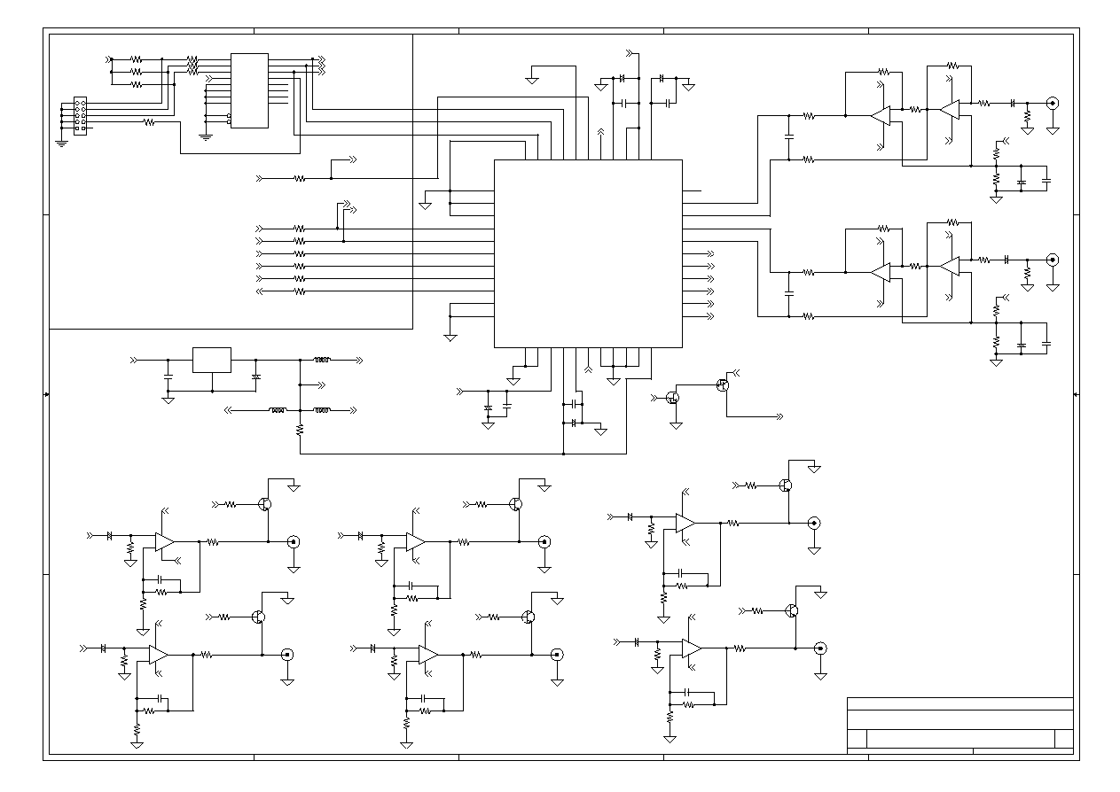
R30
2.4k
R37
4.7k
R32
4.7k
+
-
U6B
NJM5532
5
6
7
8
4
+
-
U6A
NJM5532
3
2
1
8
4
R38
470
R43
470
R42
4.7k
R44
4.7k
R51
220
TR4
2SC3327
1
3
2
R47
10k
J4
LIN
J6
ROUT1
R53
10k
+
-
U7B
NJM5532
5
6
7
8
4
R57
4.7k
TR7
2SC3327
1
3
2
R65
220
R62
10k
R68
10k
+
-
U9A
NJM5532
3
2
1
8
4
TR5
2SC3327
1
3
2
R52
220
R48
10k
R58
4.7k
TR8
2SC3327
1
3
2
R66
220
R63
10k
R69
10k
+
-
U9B
NJM5532
5
6
7
8
4
R72
4.7k
TR3
2SC3327
1
3
2
R49
220
R46
10k
R50
10k
+
-
U7A
NJM5532
3
2
1
8
4
R55
4.7k
TR6
2SC3327
1
3
2
R64
220
R61
10k
R70
4.7k
+
-
U8A
NJM5532
3
2
1
8
4
+
-
U8B
NJM5532
5
6
7
8
4
C27
0.1u
+
C34
22u
+
C37
22u
+
C38
22u
+
C35
22u
+
C36
22u
+
C33
22u
+
C15
10u
C18
0.1u
C31
0.1u
C29
0.1u
C17
0.1u
+
C32
10u
+
C16
2.2u
J5
ROUT3
R59
4.7K
R67
10k
TR2
RN1202
1
3
2
R73
4.7K
R24
(open)
U5
AK4527
1
2
3
4
5
6
7
8
9
10
11
12
13
14
15
16
17
18
19
20
21
22
23
24
25
26
27
28
29
30
31
32
33
34
35
36
37
38
39
40
41
42
43
44
SDOS
I2C
SMUTE
BICK
LRCK
SDTI1
SDTI2
SDTI3
SDTO
DAUX
DFS
DEM1
DEM0
TVDD
DVDD
DVSS
PDN
ICKS2
ICKS1
ICSK0
CAD1
CAD0
LOUT3
ROUT3
LOUT2
ROUT2
LOUT1
ROUT1
LIN-
LIN+
RIN-
RIN+
DZF2
VCOM
VREFH
AVDD
AVSS
DZF1
MCLK
P/SN
DIF0/CSN
DIF1/SCL/CCLK
LOOP0/SDA/CDTI
LOOP1
+
C30
10u
+
C25
47u
C26
0.1u
R29
4.7k
+
C21
47u
C22
0.1u
+
C23
22u
+
C19
22u
C20
1n
C24
1n
R41
(short)
J8
LOUT3
R75
4.7K
R54
10k
J9
LOUT1
J10
LOUT2
R60
4.7K
R56
4.7K
J3
RIN
R39
(open)
J7
ROUT2
+
C28
47u
C72
330p
R74
4.7K
R71
4.7k
C71
330p
C73
330p
C74
330p
C76
330p
C75
330p
L6
10u
1
2
R22470
R18470
R2551
R20470
T3
NJM78M05FA
3
2
1
OUT
GND
IN

5
5
4
4
3
3
2
2
1
1
D
D
C
C
B
B
A
A
TX
TX
V
V/TX
DA02-F
AK4112
D
AK4527
A3
2
3
Tuesday, April 18, 2000
Title
Size
Document Number
Rev
Date:
Sheet
of
TX
4112_BICK
4112_SDTO
4112_LRCK
V/TX
+3.3V
L5V
CDTI
CCLK
CSN
TX
4112_MCKO1
+12V
+3.3V
L5V
L5V
4112_MCKO2
+3.3V
CDTO
+3.3V
V/TX
4527_SDTO
PDN
T1
1:1
J1
(TX)
R2
150
R1
240
R6
1k
LE1
ERF
R7
1k
LE2
FS96
R8
1k
LE3
AUTO
LE4
V
R10
1k
R9
470
C12
0.1u
T2
LP2950A
1
2
3
OUT
GND
IN
JP2
1
2
3
C14
0.1u
C5
22p
C7
22p
+
C11
10u
+
C13
47u
C10
0.1u
U2A
74HCT14
1
2
U2B
74HCT14
3
4
U2C
74HCT14
5
6
U2D
74HCT14
9
8
L1
10u
1
2
D1
1S1588
PORT2
TORX176
1
3
4
2
6
5
OUT
VCC
GND
GND
6
5
+
C3
10u
+
C8
10u
X1
11.2896MHz
1
2
C4
0.1u
C9
0.1u
+
C1
10u
C2
0.1u
U1
AK4112A
1
2
3
4
5
6
7
8
9
10
11
12
13
14
15
16
17
18
19
20
21
22
23
24
25
26
27
28
DVDD
DVSS
TVDD
V/TX
XTI
XTO
PDN
R
AVDD
AVSS
RX1
RX2/DIF0
RX3/DIF1
RX4/DIF2
AUTO
P/SN
FS96
ERF
LRCK
SDTO
BICK
DAUX
MCKO2
MCKO1
OCKS0/CSN
OCKS1/CCLK
CM1/CDTI
CM0/CDTO
R5
18k
J2
(RX2)
R12
47k
R11
75
JP1
GND

5
5
4
4
3
3
2
2
1
1
D
D
C
C
B
B
A
A
GND
LRCK
BICK
SDTI2
SDTO
MCKO2
L
SDTI1
GND
SDTI3
4112
for 74HCT14,
74HCT541
H
DSP
DSP
DSP
4112
4112
for NJM5532 x5
for NJM5532 x5
1S1588
MCKO1
Interface
D
AKD4527
A3
3
3
Wednesday, April 19, 2000
Title
Size
Document Number
Rev
Date:
Sheet
of
SDTI3
SDTI2
SDTI1
PDN
4353_MCKI
4353_BICK
4353_LRCK
PDN
CSN
CCLK
CDTI
4112_SDTO
4112_MCKO1
L5V
L5V
L5V
L5V
4527_SDTO
+12V
-12V
4353_MCKI
4353_BICK
4353_LRCK
+12V
-12V
R76
1k
U2F
74HCT14
13
12
R77
10k
PORT5
AC3
1
2
3
4
5
6
7
8
9
10
D2
SW1
PDN
U2E
74HCT14
11
10
PORT4
TOTX176(ADC)
1
2
3
4
5
6
GND
IF
VCC
IN
5
6
U10
AK4353
1
2
3
4
5
6
7
8
9
10
11
12
13
14
15
16
17
18
19
20
21
22
23
24
MCKO
TX
DVDD
DVSS
MCKI
BICK
SDTI
LRCK
PDN
CSN
SCL/CCLK
SDA/CDTI
TST
TTL
I2C
CAD1
CAD0
AOUTR
AOUTL
VCOM
AVSS
AVDD
NC
DZF
+
C58
47u
L5
(short)
1
2
+
C47
47u
L4
(short)
1
2
+
C60
10u
C59
0.1u
C61
0.1u
+
C62
10u
+
C64
10u
C63
0.1u
+
C66
10u
C65
0.1u
+
C68
10u
C67
0.1u
C48
0.1u
+
C49
10u
+
C51
10u
C50
0.1u
+
C53
10u
C52
0.1u
C54
0.1u
+
C55
10u
+
C57
10u
C56
0.1u
C69
0.1u
C40
0.1u
C43
0.1u
+
C44
10u
C45
0.1u
+
C46
10u
C39
0.1u
C42
0.1u
+
C41
10u
R78
5.1
C70
0.1u
JP4
SDTI1
JP5
SDTI2
JP6
SDTI3


